Atomic Resolution of the graphite surface by STM (Scanning Tunneling Microscope)
Item no.: P2532000
Item no.: P2532000
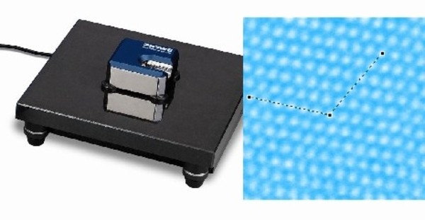
Approaching a very sharp metal tip to an electrically conductive sample by applying a electrical field leads to a current between tip and sample without any mechanical contact. This so-called tunneling current is used to investigate the electronic topography on the sub nanometer scale of a fresh prepared graphite (HOPG) surface. By scanning the tip line by line across the surface graphite atoms and the hexagonal structure are imaged.
학습목록
• Observe atoms within minutes
• Custom-designed for use in teaching labs
• Microscope consists of one compact, portable instrument, no additional instruments required
• Vibration-isolated for better and reproducible results
• Can be used both for imaging of atomic resolution and for spectroscopy
• Additional experiment with gold sample can be performed
• With interactive teaching and learning software
Tasks
1. Prepare a Pt-Ir tip and the graphite (HOPG) sample and approach the tip to the sample.
2. Investigate the topography of clean terraces and the step height between neighboring terraces in constant-current mode.
3. Image the arrangement of graphite atoms on a clean terrace by optimizing tunneling and scanning parameters. Interpret the structure by analyzing angles and distances between atoms and atomic rows and by using the 2D and 3D graphite model.
4. Measure and compare images in the constant-height and constant-current modes.
학습목록
• Tunneling effect
• Hexagonal structures
• Scanning Tunneling Microscopy (STM)
• Imaging on the sub nanometer scale
• Piezo-electric devices
• Local Density Of States (LDOS)
• Constant-Height-Mode
• Constant-Current-Mode
문의
• 제품 상담 : 직통번호(070-8645-2312)
• 팩스, 게시판, 이메일을 통해 견적문의할 수 있습니다.
견적작성 시 필요하니 성함(업체명), 연락처, 이메일 주소 등을 남겨주세요. 감사합니다.
- 이메일 : info@koreasci.com
- 팩스 : 02-929-0966
- 게시판 바로가기
배송
이 제품은 결제완료 후 해외에서 배송됩니다. 해외 물품의 재고 여부에 따라 배송기간이 달라집니다.